Acknowledgements: This equipment is financially supported by the Science and Technology Development Fund (FDCT) of Macau SAR through research project FDCT 018/2008/A. Support from the infrastructure and facility of The Institute for the Development and Quality, Macau (IDQ) is also acknowledged.
| Location | E11-G033b |
| Academic Staff in charge | Prof. Chi Tat KWOK |
| Technician | Po Kee WONG; Hou Kuan TAM |
| Telephone | (853) 8822-8042, 4291 |
Objective
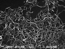
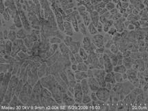
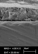
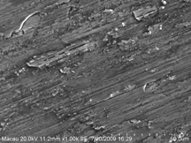
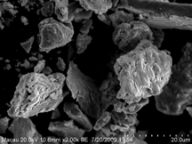
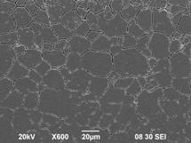
The major functions of SEM/EDS systems are to analyse the materials in the areas including microstructural analysis, failure analysis, fractography, qualitative and quantitative compositional analysis of coatings, powders, fibers and bulk materials. The SEM can allow undergraduate and research students with an interest in Materials Science to study the surface characterization and elemental compositions of materials.
Facilities
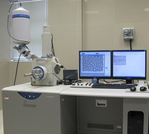
1. Scanning Electron Microscope (SEM, Hitachi S-3400N, Type I)
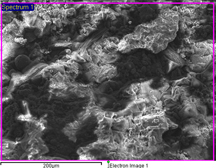
SEM is a microscope which uses electrons to form an image. It is one of the most versatile instruments for investigating the microstructure of a wide range of materials. Compared with optical microscope, SEM can offer many advantages such as larger depth of field, higher resolution and higher magnification.
Features:
- Resolution: 3 nm at 30 kV, WD = 5 mm, high vacuum mode
- Magnification range: 5 X – 300,000 X
- Specimen size: 200 mm diameter (max.)
- Max. height: 35 mm at WD = 10 mm
- SE & BSE detectors
2. Energy Dispersive X-ray Spectroscopy (EDS, Horiba EX-250)
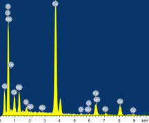
Compositional analysis in the SEM is performed by measuring the energy and intensity distribution of X-ray signal generated by a focused electron beam on the specimen. With the attachment of EDS, the precise elemental compositions of materials can be obtained with high spatial resolution.
Features:
- Quantitative analysis of elements down to boron with Si(Li) detector
- Qualitative analysis of elements by mapping and line analysis
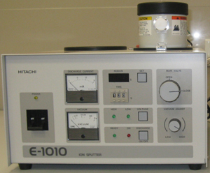
3. Ion sputter (Hitachi E1010)
For the SEM observation of non-conductive specimens such as ceramics and polymers, gold coating is required for avoiding specimens charging and keeping a high quality image. Thin layer of gold can be deposit on the specimens by the ion sputter for electrical conduction.
Experiments
Courses supported
| EMEB121 | Engineering Materials |
| EMEB351 | Advanced Materials for Engineers |
| EMEB355 | Corrosion, Wear and Degradation of Materials |
| EMEB410 | Design Projects |
| ELME702 | Physics of Materials |
| ELME717 | Special Topics in Manufacturing I: Laser Materials Processing |
| ELME718 | Special Topics in Manufacturing II : Surface Engineering |


